#FPGA Design Project Help
Explore tagged Tumblr posts
Visit Tumblr Blog
Explore Tumblr blogs with no restrictions, modern design and the best experience.
Last Seen Tumblr Blogs


Fun Fact
1,644 Tumblr posts in 1 second.
Text
OneAPI Construction Kit For Intel RISC V Processor Interface
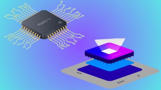
With the oneAPI Construction Kit, you may integrate the oneAPI Ecosystem into your Intel RISC V Processor.
Intel RISC-V
Recently, Codeplay, an Intel business, revealed that their oneAPI Construction Kit supports RISC-V. Rapidly expanding, Intel RISC V is an open standard instruction set architecture (ISA) available under royalty-free open-source licenses for processors of all kinds.
Through direct programming in C++ with SYCL, along with a set of libraries aimed at common functions like math, threading, and neural networks, and a hardware abstraction layer that allows programming in one language to target different devices, the oneAPI programming model enables a single codebase to be deployed across multiple computing architectures including CPUs, GPUs, FPGAs, and other accelerators.
In order to promote open source cooperation and the creation of a cohesive, cross-architecture programming paradigm free from proprietary software lock-in, the oneAPI standard is now overseen by the UXL Foundation.
A framework that may be used to expand the oneAPI ecosystem to bespoke AI and HPC architectures is Codeplay’s oneAPI Construction Kit. For both native on-host and cross-compilation, the most recent 4.0 version brings RISC-V native host for the first time.
Because of this capability, programs may be executed on a CPU and benefit from the acceleration that SYCL offers via data parallelism. With the oneAPI Construction Kit, Intel RISC V processor designers can now effortlessly connect SYCL and the oneAPI ecosystem with their hardware, marking a key step toward realizing the goal of a completely open hardware and software stack. It is completely free to use and open-source.
OneAPI Construction Kit
Your processor has access to an open environment with the oneAPI Construction Kit. It is a framework that opens up SYCL and other open standards to hardware platforms, and it can be used to expand the oneAPI ecosystem to include unique AI and HPC architectures.
Give Developers Access to a Dynamic, Open-Ecosystem
With the oneAPI Construction Kit, new and customized accelerators may benefit from the oneAPI ecosystem and an abundance of SYCL libraries. Contributors from many sectors of the industry support and maintain this open environment, so you may build with the knowledge that features and libraries will be preserved. Additionally, it frees up developers’ time to innovate more quickly by reducing the amount of time spent rewriting code and managing disparate codebases.
The oneAPI Construction Kit is useful for anybody who designs hardware. To get you started, the Kit includes a reference implementation for Intel RISC V vector processors, although it is not confined to RISC-V and may be modified for a variety of processors.
Codeplay Enhances the oneAPI Construction Kit with RISC-V Support
The rapidly expanding open standard instruction set architecture (ISA) known as RISC-V is compatible with all sorts of processors, including accelerators and CPUs. Axelera, Codasip, and others make Intel RISC V processors for a variety of applications. RISC-V-powered microprocessors are also being developed by the EU as part of the European Processor Initiative.
At Codeplay, has been long been pioneers in open ecosystems, and as a part of RISC-V International, its’ve worked on the project for a number of years, leading working groups that have helped to shape the standard. Nous realize that building a genuinely open environment starts with open, standards-based hardware. But in order to do that, must also need open hardware, open software, and open source from top to bottom.
This is where oneAPI and SYCL come in, offering an ecosystem of open-source, standards-based software libraries for applications of various kinds, such oneMKL or oneDNN, combined with a well-developed programming architecture. Both SYCL and oneAPI are heterogeneous, which means that you may create code once and use it on any GPU AMD, Intel, NVIDIA, or, as of late, RISC-V without being restricted by the manufacturer.
Intel initially implemented RISC-V native host for both native on-host and cross-compilation with the most recent 4.0 version of the oneAPI Construction Kit. Because of this capability, programs may be executed on a CPU and benefit from the acceleration that SYCL offers via data parallelism. With the oneAPI Construction Kit, Intel RISC V processor designers can now effortlessly connect SYCL and the oneAPI ecosystem with their hardware, marking a major step toward realizing the vision of a completely open hardware and software stack.
Read more on govindhtech.com
#OneAPIConstructionKit#IntelRISCV#SYCL#FPGA#IntelRISCVProcessorInterface#oneAPI#RISCV#oneDNN#oneMKL#RISCVSupport#OpenEcosystem#technology#technews#news#govindhtech
2 notes
·
View notes
Text
FPGA Market - Exploring the Growth Dynamics

The FPGA market is witnessing rapid growth finding a foothold within the ranks of many up-to-date technologies. It is called versatile components, programmed and reprogrammed to perform special tasks, staying at the fore to drive innovation across industries such as telecommunications, automotive, aerospace, and consumer electronics. Traditional fixed-function chips cannot be changed to an application, whereas in the case of FPGAs, this can be done. This brings fast prototyping and iteration capability—extremely important in high-flux technology fields such as telecommunications and data centers. As such, FPGAs are designed for the execution of complex algorithms and high-speed data processing, thus making them well-positioned to handle the demands that come from next-generation networks and cloud computing infrastructures.
In the aerospace and defense industries, FPGAs have critically contributed to enhancing performance in systems and enhancing their reliability. It is their flexibility that enables the realization of complex signal processing, encryption, and communication systems necessary for defense-related applications. FPGAs provide the required speed and flexibility to meet the most stringent specifications of projects in aerospace and defense, such as satellite communications, radar systems, and electronic warfare. The ever-improving FPGA technology in terms of higher processing power and lower power consumption is fueling demand in these critical areas.
Consumer electronics is another upcoming application area for FPGAs. From smartphones to smart devices, and finally the IoT, the demand for low-power and high-performance computing is on the rise. In this regard, FPGAs give the ability to integrate a wide array of varied functions onto a single chip and help in cutting down the number of components required, thereby saving space and power. This has been quite useful to consumer electronics manufacturers who wish to have state-of-the-art products that boast advanced features and have high efficiency. As IoT devices proliferate, the role of FPGAs in this area will continue to foster innovation.
Growing competition and investments are noticed within the FPGA market, where key players develop more advanced and efficient products. The performance of FPGAs is increased by investing in R&D; the number of features grows, and their cost goes down. This competitive environment is forcing innovation and a wider choice availability for end-users is contributing to the growth of the whole market.
Author Bio -
Akshay Thakur
Senior Market Research Expert at The Insight Partners
2 notes
·
View notes
Text
Boost Your VLSI Career with the Best Training Institutes in Bangalore
The Rising Demand for VLSI Professionals With the exponential growth of the semiconductor industry, VLSI (Very Large Scale Integration) design has emerged as one of the most in-demand fields in electronics and embedded systems. From smartphones and computers to self-driving cars and smart appliances, VLSI technology plays a crucial role in enabling intelligent digital systems. Due to the increasing dependency on integrated circuits in almost every electronic device, there is a rising need for skilled VLSI professionals. This demand has led many aspiring engineers to seek quality training from reputed institutes in Bangalore, India’s hub for technology and innovation.
Why Bangalore is the Preferred Destination for VLSI Training Bangalore, often called the Silicon Valley of India, is home to numerous semiconductor companies, design houses, and electronics manufacturing firms. This environment creates ample opportunities for practical exposure and industry collaboration. Among the top vlsi institutes in bangalore, candidates can find a range of training programs that combine theoretical knowledge with hands-on lab experience. These institutes offer specialized courses in areas like digital design, physical design, ASIC verification, and FPGA implementation, catering to the evolving needs of the industry. Choosing the right institute in Bangalore gives learners a valuable edge in both knowledge and employment prospects.
Features of an Effective VLSI Training Program An ideal VLSI training program is structured to provide not only strong foundational concepts but also practical exposure using real-time tools and industry-standard software. Courses designed in alignment with current job roles help learners understand design flows, verification methodologies, and layout processes. Instructors with industry experience and the availability of live projects further enhance the learning experience. Institutes that offer placement support, interview preparation, and resume guidance are often preferred by candidates aiming for a stable career in VLSI.
The Role of VLSI Training in Career Advancement Fresh graduates and working professionals who wish to enter the semiconductor domain can significantly benefit from VLSI training. These programs are crafted to develop technical proficiency and make learners job-ready. Bangalore provides a dynamic setting where individuals can access the latest tools, interact with domain experts, and build a professional network. A focused VLSI training program in this city can open the door to numerous job opportunities in top semiconductor firms.
Choosing a Job-Oriented VLSI Institute Enrolling in a job oriented vlsi training institute in bangalore can be a game-changer for anyone aiming to enter the core electronics field. Such institutes focus on equipping students with industry-relevant skills and practical expertise, thus improving their employability. These job-oriented programs emphasize real-world applications, timely projects, and guidance that align with current hiring trends in the VLSI sector.
Conclusion VLSI is a promising field with ever-expanding opportunities. For aspiring engineers looking to start or grow their careers in this domain, choosing the right training institute is critical. Bangalore stands out as a prime destination due to its strong industry presence and top-quality education providers. One of the most trusted names in this space is Takshila Institute of VLSI Technologies, known for offering robust, industry-aligned training. From comprehensive curriculum to placement support, the right institute can significantly impact an individual's career path. In conclusion, selecting the best institute from the top vlsi institutes in bangalore or opting for a job oriented vlsi training institute in bangalore can be the key step toward a successful future in the semiconductor industry.
0 notes
Text
Designing the Future: How Embedded Systems Enhance Medical Device Reliability
Technology is making a huge impact in healthcare, and at the core of many of those breakthroughs is smart engineering. Voler Systems has become a trusted name in developing medical technologies that help people live healthier, safer lives. Whether it's designing advanced medical devices, building embedded systems, or creating custom FPGA solutions, Voler Systems is helping bring the future of healthcare to life.

Turning Ideas Into Life-Saving Medical Devices Bringing a medical device to market is about more than just having a great idea—it requires deep technical knowledge, strict regulatory compliance, and careful planning. Voler Systems specializes in medical devices development, working closely with clients from early design to final production. Their team understands the high stakes involved and focuses on building devices that are accurate, reliable, and user-friendly. Whether it’s for remote patient monitoring or in-clinic diagnostic equipment, their experience helps turn concepts into real-world healthcare solutions. To learn more, visit the Medical Devices Development page.
Reliable Embedded Systems That Power Healthcare Devices Behind most smart medical devices is a powerful system running in the background. These systems are known as embedded systems—and getting them right is critical. Voler Systems has led numerous projects in embedded systems, creating customized designs that power everything from wearable monitors to imaging machines. The focus is always on low power usage, fast response time, and reliability in demanding healthcare settings. Find out how embedded tech powers medical innovation at Projects Embedded Systems.
Smarter Hardware with FPGA Development In situations where performance and speed are non-negotiable, FPGAs (Field Programmable Gate Arrays) provide a unique advantage. These reprogrammable chips allow for fast, custom hardware-level functionality—ideal for critical healthcare applications. Voler Systems offers expert FPGA development services, helping healthcare companies create high-performance systems for imaging, diagnostics, and real-time processing. Explore the possibilities at FPGA Development.
A Trusted Technology Partner in Healthcare Developing smart medical technologies requires more than just technical skills—it requires a deep understanding of both engineering and healthcare needs. That’s where Voler Systems stands out. Whether it’s creating intelligent devices, building efficient embedded platforms, or accelerating performance with FPGA solutions, their work helps healthcare innovators bring safe and effective products to life.
If you're looking to bring a new medical product to market—or improve an existing one—Voler Systems offers the engineering expertise and industry knowledge to help make it happen.
#wearable medical device#electronic design services#medical device design#embedded systems design#projects embedded systems#medical device development company
0 notes
Text

FPGA Assignment Help. FPGA Project Help. FPGA Homework Help
An FPGA (Field Programmable Gate Array) is an integrated circuit that can be programmed by the user after manufacturing to perform specific digital functions. Unlike fixed-function chips, FPGAs contain an array of configurable logic blocks and interconnects that allow designers to create custom hardware circuits.
Some of the important vendors of FPGA are:
Xilinx FPGA (now part of AMD)
Intel (formerly Altera)
Lattice Semiconductor FPGA
Get in touch with us for expert assistance for any FPGA assignment, project or homework. Our solutions are fast and accurate.
Visit our website for more information or email us at [email protected]. You can also ping us on Whatsapp on +1.289.499.9269 for instant support.
0 notes
Text
Master ASIC Design and Verification Training Today

In today’s fast-paced semiconductor industry, mastering ASIC (Application-Specific Integrated Circuit) design and verification is essential for engineers and professionals looking to advance their careers. With cutting-edge technology and increasing demand for customized chip designs, the need for skilled ASIC designers is greater than ever. If you are eager to enhance your expertise, ASIC Design and Verification Training is the perfect opportunity to gain in-depth knowledge and practical skills.
Why Choose ASIC Design and Verification Training?
ASIC design is a complex yet rewarding field that requires a deep understanding of digital circuits, system architecture, and verification methodologies. This training equips you with:
Fundamental and Advanced ASIC Design Concepts – Learn the principles of ASIC development, from design to implementation.
Verification Techniques – Master simulation-based verification, formal verification, and functional testing.
Industry-Standard Tools – Get hands-on experience with tools like Verilog, VHDL, SystemVerilog, and UVM.
Practical Projects and Case Studies – Work on real-world projects to strengthen your problem-solving abilities.
Expert Guidance – Learn from industry professionals with years of experience in ASIC design and verification.
Who Should Enroll?
This training is ideal for:
Engineering students and graduates looking to specialize in VLSI and ASIC design.
Working professionals aiming to upskill in semiconductor design.
Anyone passionate about learning digital design and verification methodologies.
Career Benefits of ASIC Design and Verification Online Training
With expertise in ASIC design and verification, you can unlock various career opportunities in semiconductor and electronics industries. Job roles include:
ASIC Design Engineer
Verification Engineer
FPGA Engineer
VLSI Design Engineer
Embedded Systems Engineer
Enroll Today and Advance Your Career!
Don’t miss the chance to boost your career in the high-demand field of ASIC design. Join ASIC Design and Verification Training today and gain the skills needed to thrive in the semiconductor industry. Start your journey towards success with expert-led training and hands-on experience.
At Multisoft Virtual Academy, we provide comprehensive training programs to help tech enthusiasts achieve professional excellence. Sign up now and take the next step in your career!
0 notes
Text
Takshila Institute of VLSI Technologies: A Top Choice for DFT and FPGA Design Training
In the ever-evolving semiconductor industry, mastering Design for Testability (DFT) and FPGA design is essential for engineers seeking to build successful careers. Among the top 10 DFT training institutes and premier FPGA design institutes in Bangalore, the Takshila Institute of VLSI Technologies in India has established itself as a trusted name, offering industry-relevant courses to empower aspiring professionals.
The DFT training program at Takshila Institute is meticulously designed to provide students with a comprehensive understanding of test methodologies, scan architecture, boundary scan, ATPG (Automatic Test Pattern Generation), and fault simulation. With a focus on hands-on learning, the program equips students with practical skills to implement efficient and cost-effective testing techniques. By utilizing state-of-the-art tools and technologies, participants gain real-world experience, making them job-ready for roles in leading semiconductor companies.
Similarly, the FPGA design training program at the institute is tailored to address the needs of students and professionals aiming to specialize in field-programmable gate arrays. The course covers critical topics, including digital design, RTL coding, synthesis, and hardware debugging. Students work with industry-standard tools to design, simulate, and implement FPGA-based systems, ensuring they are well-prepared to tackle real-world challenges in FPGA design.
What sets the Takshila Institute of VLSI Technologies apart is its commitment to quality education and industry alignment. The institute’s highly experienced faculty members bring decades of expertise to the classroom, ensuring that students receive guidance from professionals who understand the nuances of DFT and FPGA design. The programs also emphasize project-based learning, allowing students to apply theoretical knowledge to practical scenarios.
Takshila Institute’s focus on placement support further enhances its reputation among the top 10 DFT training institutes and leading FPGA design institutes in Bangalore. The institute has built strong industry connections, helping students secure internships and full-time roles in prominent semiconductor companies. Through resume-building workshops, mock interviews, and career counseling, participants are well-prepared to take the next step in their careers.
By choosing Takshila Institute, students gain access to robust training programs, expert mentorship, and unparalleled industry exposure. Whether you aspire to excel in DFT training or FPGA design, the institute provides the perfect platform to achieve your goals.
Embark on your journey to success with the Takshila Institute of VLSI Technologies, a leading name in DFT and FPGA design training in India. Your future in the semiconductor industry begins here.
1 note
·
View note
Text
Agilex 3 FPGAs: Next-Gen Edge-To-Cloud Technology At Altera
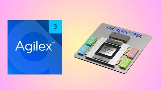
Agilex 3 FPGA
Today, Altera, an Intel company, launched a line of FPGA hardware, software, and development tools to expand the market and use cases for its programmable solutions. Altera unveiled new development kits and software support for its Agilex 5 FPGAs at its annual developer’s conference, along with fresh information on its next-generation, cost-and power-optimized Agilex 3 FPGA.
Altera
Why It Matters
Altera is the sole independent provider of FPGAs, offering complete stack solutions designed for next-generation communications infrastructure, intelligent edge applications, and high-performance accelerated computing systems. Customers can get adaptable hardware from the company that quickly adjusts to shifting market demands brought about by the era of intelligent computing thanks to its extensive FPGA range. With Agilex FPGAs loaded with AI Tensor Blocks and the Altera FPGA AI Suite, which speeds up FPGA development for AI inference using well-liked frameworks like TensorFlow, PyTorch, and OpenVINO toolkit and tested FPGA development flows, Altera is leading the industry in the use of FPGAs in AI inference workload
Intel Agilex 3
What Agilex 3 FPGAs Offer
Designed to satisfy the power, performance, and size needs of embedded and intelligent edge applications, Altera today revealed additional product details for its Agilex 3 FPGA. Agilex 3 FPGAs, with densities ranging from 25K-135K logic elements, offer faster performance, improved security, and higher degrees of integration in a smaller box than its predecessors.
An on-chip twin Cortex A55 ARM hard processor subsystem with a programmable fabric enhanced with artificial intelligence capabilities is a feature of the FPGA family. Real-time computation for time-sensitive applications such as industrial Internet of Things (IoT) and driverless cars is made possible by the FPGA for intelligent edge applications. Agilex 3 FPGAs give sensors, drivers, actuators, and machine learning algorithms a smooth integration for smart factory automation technologies including robotics and machine vision.
Agilex 3 FPGAs provide numerous major security advancements over the previous generation, such as bitstream encryption, authentication, and physical anti-tamper detection, to fulfill the needs of both defense and commercial projects. Critical applications in industrial automation and other fields benefit from these capabilities, which guarantee dependable and secure performance.
Agilex 3 FPGAs offer a 1.9×1 boost in performance over the previous generation by utilizing Altera’s HyperFlex architecture. By extending the HyperFlex design to Agilex 3 FPGAs, high clock frequencies can be achieved in an FPGA that is optimized for both cost and power. Added support for LPDDR4X Memory and integrated high-speed transceivers capable of up to 12.5 Gbps allow for increased system performance.
Agilex 3 FPGA software support is scheduled to begin in Q1 2025, with development kits and production shipments following in the middle of the year.
How FPGA Software Tools Speed Market Entry
Quartus Prime Pro
The Latest Features of Altera’s Quartus Prime Pro software, which gives developers industry-leading compilation times, enhanced designer productivity, and expedited time-to-market, are another way that FPGA software tools accelerate time-to-market. With the impending Quartus Prime Pro 24.3 release, enhanced support for embedded applications and access to additional Agilex devices are made possible.
Agilex 5 FPGA D-series, which targets an even wider range of use cases than Agilex 5 FPGA E-series, which are optimized to enable efficient computing in edge applications, can be designed by customers using this forthcoming release. In order to help lower entry barriers for its mid-range FPGA family, Altera provides software support for its Agilex 5 FPGA E-series through a free license in the Quartus Prime Software.
Support for embedded applications that use Altera’s RISC-V solution, the Nios V soft-core processor that may be instantiated in the FPGA fabric, or an integrated hard-processor subsystem is also included in this software release. Agilex 5 FPGA design examples that highlight Nios V features like lockstep, complete ECC, and branch prediction are now available to customers. The most recent versions of Linux, VxWorks, and Zephyr provide new OS and RTOS support for the Agilex 5 SoC FPGA-based hard processor subsystem.
How to Begin for Developers
In addition to the extensive range of Agilex 5 and Agilex 7 FPGAs-based solutions available to assist developers in getting started, Altera and its ecosystem partners announced the release of 11 additional Agilex 5 FPGA-based development kits and system-on-modules (SoMs).
Developers may quickly transition to full-volume production, gain firsthand knowledge of the features and advantages Agilex FPGAs can offer, and easily and affordably access Altera hardware with FPGA development kits.
Kits are available for a wide range of application cases and all geographical locations. To find out how to buy, go to Altera’s Partner Showcase website.
Read more on govindhtech.com
#Agilex3FPGA#NextGen#CloudTechnology#TensorFlow#Agilex5FPGA#OpenVINO#IntelAgilex3#artificialintelligence#InternetThings#IoT#FPGA#LPDDR4XMemory#Agilex5FPGAEseries#technology#Agilex7FPGAs#QuartusPrimePro#technews#news#govindhtech
2 notes
·
View notes
Text
Takshila Institute of VLSI Technologies: Premier Verilog Training Institute in India
Verilog, a hardware description language (HDL), is fundamental in the design and development of digital systems, including microprocessors, FPGAs, and ASICs. Aspiring VLSI professionals often seek comprehensive training in Verilog to establish a strong foundation in digital design. Among the top choices for this specialized education is the Takshila Institute of VLSI Technologies, a renowned name in India offering exceptional Verilog training. Whether you're in Hyderabad or Bangalore, Takshila Institute stands out as a premier destination for mastering Verilog.
Takshila Institute’s Verilog training program is meticulously crafted to cater to students, fresh graduates, and working professionals. The course begins with the basics of digital design and progresses to advanced concepts, including combinational and sequential logic, testbenches, and synthesis. The curriculum emphasizes practical learning, allowing students to work on real-world design projects and understand how Verilog is used in creating functional digital systems.
One of the standout features of Takshila’s Verilog training is the hands-on experience it provides. Students gain expertise in writing, simulating, and debugging Verilog code using industry-standard tools such as Cadence and Synopsys. This practical exposure ensures learners can confidently apply their skills in professional environments. The program also includes modules on advanced design techniques, preparing students to tackle complex challenges in the VLSI domain.
The institute’s faculty comprises seasoned professionals with extensive experience in digital design and verification. Their personalized mentoring approach helps students grasp even the most challenging concepts with ease. Through interactive sessions and real-world examples, the faculty ensures that learners develop both theoretical knowledge and practical proficiency in Verilog.
Another advantage of choosing Takshila Institute is its strong placement support. The institute has established partnerships with leading semiconductor companies, enabling students to secure internships and full-time positions. Its dedicated placement team conducts mock interviews, resume-building workshops, and career counseling sessions, ensuring students are well-prepared for job opportunities in the VLSI sector.
Takshila Institute also caters to diverse learning needs by offering online verification training. This flexibility allows students from across India to access high-quality education without geographical constraints. Whether you are in Hyderabad, Bangalore, or any other part of the country, you can benefit from Takshila’s expert-led training programs.
In conclusion, the Takshila Institute of VLSI Technologies is a top-tier choice for those seeking Verilog training institutes in Bangalore. With its industry-aligned curriculum, experienced faculty, practical focus, and strong placement support, Takshila empowers students to excel in digital design and achieve their career goals in the VLSI industry.
0 notes
Text
Takshila Institute of VLSI Technologies – The Best VLSI Training Institute in India
The VLSI (Very Large Scale Integration) industry is one of the fastest-growing fields in semiconductor technology, creating numerous job opportunities for skilled professionals. To build a successful career in VLSI design and verification, it is essential to receive training from a reputed institute that offers industry-focused courses, hands-on experience, and expert mentorship.
The Takshila Institute of VLSI Technologies is recognized as the best VLSI training institute in India, providing comprehensive courses for students and working professionals. With cutting-edge lab facilities, real-time projects, and expert faculty, this institute equips learners with the knowledge and skills required to excel in the semiconductor industry.
For those looking for flexible learning options, the institute also offers Online VLSI Courses, making quality education accessible from anywhere. The Online VLSI Courses at Takshila Institute of VLSI Technologies are designed to meet the needs of students and professionals who want to upgrade their skills while balancing work or academic commitments. The courses cover essential topics like RTL design, verification methodologies, FPGA design, DFT (Design for Testability), and physical design. With live interactive sessions, recorded lectures, and hands-on projects, learners gain practical exposure to VLSI tools and techniques used in the industry.
What makes Takshila Institute of VLSI Technologies the best VLSI training institute in India is its structured curriculum, industry partnerships, and placement assistance. The training programs are designed to bridge the gap between academia and industry, ensuring that students acquire job-ready skills. The faculty consists of experienced VLSI professionals who provide insights into real-world chip design challenges. Moreover, the institute has strong industry connections, helping students secure high-paying jobs in top semiconductor companies.
The online vlsi courses in bangalore offered by Takshila Institute of VLSI Technologies provide learners with the flexibility to study from home while gaining practical experience through virtual labs and project-based learning. The institute uses industry-standard tools and offers mentorship programs to help students gain technical expertise and problem-solving skills.
For students and professionals looking to build a successful career in VLSI design and verification, enrolling at Takshila Institute of VLSI Technologies is a strategic choice. Whether attending classroom training or online courses, learners receive top-quality education, hands-on experience, and career support. With the growing demand for VLSI engineers, this training opens doors to exciting job opportunities in the semiconductor industry.
By choosing Takshila Institute of VLSI Technologies, students gain a competitive edge in VLSI design, verification, and semiconductor technology, paving the way for a successful and rewarding career.
0 notes
Text
Mastering VLSI: Why the Right Training Matters for a Thriving Tech Career
The Rising Demand for VLSI Experts The modern world is driven by electronics. From smartphones to smart cars, every innovation depends on microchips designed using VLSI (Very Large Scale Integration) technology. With the growing use of AI, IoT, and automation, the need for skilled VLSI professionals has increased rapidly. This makes VLSI an essential field for those looking to build a strong career in electronics and semiconductor industries. Choosing the right learning path is key to making the most of this opportunity.
Exploring the Benefits of VLSI Online Training Courses Many learners today seek flexible and effective ways to upskill. VLSI online training courses offer an excellent solution by combining convenience with quality education. These courses provide access to experienced instructors, practical assignments, and industry-based projects—all from the comfort of home. Learners can grasp digital design, physical design, verification, and ASIC/FPGA concepts without sacrificing their job or academic responsibilities. The online model also allows repeated learning and flexible scheduling, making it ideal for beginners as well as professionals wanting to upgrade their knowledge.
Choosing the Right Learning Mode While online learning provides flexibility, some individuals prefer classroom-based teaching for real-time interaction and immediate doubt clearing. The choice between online and offline modes largely depends on individual preferences, learning habits, and career goals. However, what truly matters is the quality of the training and the expertise of the instructors involved.
Key Skills Taught in VLSI Training A well-structured VLSI course should cover areas like CMOS technology, HDL languages such as Verilog and VHDL, physical design flow, and functional verification techniques. Practical exposure through lab sessions or simulation tools is crucial. Additionally, learners should be guided on real-time projects to apply their theoretical knowledge to industry problems.
Why VLSI Coaching in Hyderabad is Gaining Popularity Hyderabad has become a major hub for semiconductor and electronics industries. As a result, VLSI coaching in Hyderabad has gained recognition for producing skilled professionals. Reputed training centers in the city offer tailored coaching with an industry-aligned curriculum, experienced faculty, and placement support. Many aspirants from across the country travel to Hyderabad to benefit from this coaching environment that bridges academic learning with industry demands.
Conclusion VLSI technology plays a vital role in shaping the electronics and semiconductor industries. Whether through VLSI online training courses or classroom-based programs like VLSI coaching in Hyderabad, acquiring the right skills is essential for career growth. Institutions like Takshila Institute of VLSI Technologies provide training that matches industry standards, helping learners succeed in a competitive field. The choice of platform and location may differ, but the goal remains the same—building a strong foundation in VLSI for a successful future.
0 notes
Text
VLSI, CSE, Embedded Systems, Matlab & EEE Engineering Projects
Perhaps you are seeking some content or information regarding VLSI, CSE, Embedded Systems, MATLAB & EEE Engineering Projects. Here’s a possible approach depending on your needs:
1. Promotional Content:
Want to find the best Engineering projects in VLSI, CSE, Embedded Systems, MATLAB or EEE? Takeoffprojects provides consultancy and assistance to help realise your academic concepts from concept to reality. Come to Tirupati and learn, build, and showcase your expertise through real time projects!
2. List of Project Topics
VLSI: Low power design circuits, FPGA based signal processing and the like.
CSE: AI/ML apps, blockchain, web app, etc.
Embedded Systems: Smart technology, humans, Computers, Internet of Things, Automation, Robotics, Smart homes and buildings, etc.
MATLAB: Image processing, signal processing, control systems, and such like.
EEE: Renewable power systems & architectures, smart electricity grid, power conversion, etc.
3. Project Offer Details
Takeoffprojects provide exclusive, unique and practical academic projects for students in VLSI, CSE, Embedded systems MATLAB and EEE. Expert advice, real project documentation, live project demos in Tirupati.
If any of these sparks an idea for a particular type of content such as a post, a brochure or an ad feel free to let me know, otherwise if you would like me to elaborate on any of the above notions please do.
#engineering#projects#cse#vlsi#smartproject#computers#eee#embedded#matlab#takeoffprojects#takeoffedugroup
0 notes
Text
How the Best ECE Colleges in Bhopal Prepare Students for Global Careers

electronics engineer
As a professor of Electronics & Communication Engineering (ECE) in Bhopal, I have observed how technology has reshaped industries worldwide. Electronics & Communication Engineering is no longer limited to circuit design or telecommunications—it has expanded into Artificial Intelligence (AI), Internet of Things (IoT), 5G, robotics, and semiconductor technology.
For students aspiring to pursue global careers, choosing the right ECE college in Bhopal is crucial. The best institutions provide a strong academic foundation, hands-on experience, industry exposure, and international collaborations that prepare students for global job opportunities.
In this blog, I will explore how the best Electronics & Communication Engineering college in Bhopal equip students for successful careers in multinational companies, research institutions, and tech startups across the world.
Why ECE Graduates Are in High Demand Globally?
The global demand for Electronics & Communication Engineers has surged due to advancements in:
✔ 5G & Wireless Communication – The global 5G market is expected to reach $667 billion by 2026 ✔ Semiconductor Industry Growth – With countries investing in local chip manufacturing, the global semiconductor market is projected to exceed $1 trillion by 2030 ✔ AI & IoT Integration – Smart cities, automation, and AI-driven applications are creating millions of jobs in AI-powered ECE fields ✔ Electric Vehicles & Automation – Companies like Tesla, Tata Motors, and Bosch need engineers with expertise in embedded systems, power electronics, and automation
With top ECE colleges in Bhopal aligning their curricula with global trends, students have excellent opportunities to work in the USA, Germany, Japan, South Korea, and the Middle East.
How the Best ECE Colleges in Bhopal Prepare Students for Global Careers?
1. Internationally Aligned Curriculum & Specializations
A globally competitive Electronics & Communication Engineering curriculum must cover:
5G & Wireless Communication – To develop expertise in telecom, networking, and RF engineering
Embedded Systems & IoT – For careers in smart devices, home automation, and industrial IoT
VLSI & Semiconductor Technology – Essential for jobs in chip design and semiconductor fabrication
AI & Machine Learning for ECE – For applications in autonomous vehicles, AI-based signal processing, and robotics
Cybersecurity in Communication Networks – Critical for protecting data transmission across global telecom networks
At Rabindranath Tagore University (RNTU) Bhopal, the B.Tech in ECE integrates AI-driven automation, IoT applications, and advanced chip design, ensuring students are industry-ready for global markets.
2. International Industry Tie-ups & Internships
The best ECE colleges in Bhopal have partnerships with leading global companies such as:
✔ Texas Instruments, Qualcomm, and Intel – For VLSI & chip design careers ✔ Ericsson, Nokia, and Huawei – For 5G & telecom network roles ✔ Bosch, Honeywell, and Schneider Electric – For IoT & automation applications ✔ Tesla, Tata Motors, and Mahindra Electric – For electric vehicle technology
At RNTU Bhopal, students gain hands-on experience through internships and training programs with top tech firms. These industry collaborations help students develop practical skills and secure global placements.
3. Advanced Research Labs & International Certifications
Having state-of-the-art laboratories is essential for global career preparation. The best ECE colleges in Bhopal provide:
🔹 VLSI & FPGA Labs – Training students in chip design and hardware implementation 🔹 Embedded Systems & IoT Labs – Working on real-world automation and smart device projects 🔹 5G Wireless Communication Labs – Developing skills in RF design, antenna testing, and telecom networking 🔹 AI & Signal Processing Labs – Applying machine learning in image and speech processing
At RNTU Bhopal, students receive certifications in AI, IoT, VLSI, and cybersecurity, making them highly employable in international job markets.
4. Global Placement Opportunities
A major factor in choosing the best ECE college in Bhopal is placement assistance for international careers. The top colleges provide:
✅ Training in global job market trends & interview preparation ✅ Connections with top recruiters from the USA, Europe, and Asia ✅ Opportunities to work on international research projects
At RNTU Bhopal, students receive dedicated career counseling and placement support, helping them secure high-paying jobs in multinational companies.
5. Higher Education & International Collaborations
The best ECE colleges in Bhopal support students pursuing higher studies at top international universities. Many students go on to pursue:
Master’s & Ph.D. programs in AI, IoT, and VLSI at universities like MIT, Stanford, and TU Munich
Scholarship programs for higher education in the USA, Canada, and Germany
Global research collaborations with institutions such as ISRO, NASA, and CERN
At RNTU Bhopal, students have access to international exchange programs, scholarships, and collaborative research opportunities with global universities.
Why RNTU Bhopal Stands Out as the Best ECE College for Global Careers?
Among all the top ECE colleges in Bhopal, Rabindranath Tagore University (RNTU) offers:
✔ A globally competitive ECE curriculum ✔ Hands-on training with international tech companies ✔ Industry certifications & research collaborations ✔ Strong global placement support
Conclusion: Choose the Right ECE College for a Global Career
If you aspire to work in multinational tech firms, global telecom companies, or AI-driven automation industries, choosing the right ECE college in Bhopal is critical. The best ECE institutions provide:
✔ World-class education & industry-relevant training ✔ Research opportunities & global industry tie-ups ✔ High-tech labs & advanced certifications ✔ Placement support with international companies
Among the best ECE colleges in Bhopal, Rabindranath Tagore University (RNTU) Bhopal stands out as the top choice for students looking to build global careers in Electronics & Communication Engineering.
0 notes
Text
Best VLSI Projects for ECE Students
Very Large Scale Integration (VLSI) is a crucial domain in Electronics and Communication Engineering (ECE), offering opportunities to design and develop microchips and complex electronic circuits. Here are some of the best VLSI project ideas for ECE students that can enhance their knowledge and career prospects:

FPGA-Based System Design: Field-Programmable Gate Arrays (FPGAs) are widely used in the industry for prototyping. Students can design a system using FPGA for applications such as real-time video processing, digital signal processing, or cryptography.
Low-Power VLSI Design: With the growing demand for energy-efficient devices, low-power VLSI design projects like creating low-power adders, multipliers, or memory circuits can be impactful and highly relevant.
ASIC Design for IoT Applications: Application-Specific Integrated Circuits (ASICs) are tailored for specific purposes. Designing ASICs for IoT devices, such as smart sensors or wearable technology, is a cutting-edge project idea.
Digital Signal Processing (DSP) Architecture: DSP is critical for applications like audio processing, image processing, and telecommunications. Implementing DSP algorithms on VLSI platforms offers practical insights.
High-Speed Processor Design: Designing processors with high-speed operation and reduced latency is a challenging yet rewarding project. Focus on architectures like RISC or multi-core processors.
Memory Design and Optimization: Projects focusing on memory units such as SRAM, DRAM, or Flash memory can help students understand memory hierarchy, speed, and power trade-offs.
Verification and Testing of VLSI Circuits: Verification ensures the accuracy of designs before fabrication. Projects in this area can include creating automated verification environments using tools like Verilog or SystemVerilog.
By undertaking these projects, students not only gain technical expertise but also develop problem-solving and analytical skills, preparing them for a thriving career in the VLSI industry.
#VLSI Projects#Engineering Projects#Final Year Projects#VLSI Final Year Projects#Btech Projects Major Projects#VLSI Major Projects
0 notes
Text
Vivado Support with IDesignSpec Suite- Agnisys
IDesignSpecTM (IDS) is a product suite that improves the productivity of FPGA/ASIC, IP/SoC, and system development teams. These products encompass an innovative register information management system to capture hardware functional specifications and addressable register specifications in a single executable specification. All downstream code and documentation for the addressable registers, sequences, or interrupts can be generated from this single specification along with validation in Xilinx Vivado Environment.
Vivado is a tool developed by Xilinx for creating digital designs. Vivado facilitates developers checking their designed RTL correctness and validating it in a hardware platform with different vendor’s boards containing Xilinx FPGAs. Currently, Zynq7000 family is used like Artix-7, Kintex-7 etc.. These special devices have two parts, the Programmable Logic (PL) block and the Processing System (PS) block. PL is used to implement RTL and PS is used for embedded applications oriented to ARM processors using Embedded C.
The following problems can be solved by IDesignSpec when generating outputs for Vivado:
Simplified RTL implementation:
Users do not need to worry about the RTL implementation. IDS takes care of generating the necessary RTL code.
Pre-validated RTL:
Users do not need to validate the RTL at their end because the IDS-generated RTL is already validated.
The following process achieves these results.
As shown in Figure 1 below, RTL output can be generated by the Agnisys cross platform GUI by going to the configuration window and selecting the desired output:
Users can generate the following two files from IDesignSpec:
RTL output file
AXI widget file
Flow of Process Execution:
This process is divided into two parts:
Create package IP
Generate bitstream with Zynq Processing System
Create Package IP:
The process to create package IP is shown below
Generate Bitstream:
Generate the bitstream with Zynq Processing System as shown below:
The generated bitstream is used to program the FPGA and run on the hardware. Vivado is built with an SDK for running projects based on C applications.
Application Example:
A typical application on the hardware platform, Zedboard, using both Vivado and SDK with IDesignSpec-GDI and IDS-Validate is shown below:
Action register, extra register, parity, and sniffer code are generated by IDS.
Cosmic code, which is hard-coded, will induce errors in registers through the switch.
Parity and sniffer will detect errors in registers and send a signal to an error LED. This is part of the Vivado implementation.
IDS-Validate generated C files are executed by the Zynq Processor through the Software AXI Interface, sending signals to the PCB according to the application. This is part of the SDK.
Conclusion:
With the help of the IDesignSpec Suite, users can create embedded projects very easily. There is no burden of writing HDL files and C programs for specific application projects.
Call for action: To get more information about how we can help you to create Vivado-based projects reach out here.
0 notes
Text
Unlocking the Power of Xilinx FPGAs: A Comprehensive Guide to Architecture, Series, and Implementation
Introduction to FPGAs
Field-Programmable Gate Arrays (FPGAs) are a unique class of reprogrammable silicon devices that allow for custom hardware implementations after manufacturing. Unlike traditional processors, FPGAs are composed of configurable logic blocks, memory elements, and routing resources, enabling users to create circuits tailored to specific needs. This flexibility is ideal for applications that require real-time data processing, parallel computing, or low-latency performance, such as telecommunications, automotive systems, and artificial intelligence (AI).
FPGAs differ fundamentally from traditional CPUs and GPUs, which execute instructions in a predefined sequence. With FPGAs, developers can define custom data paths that operate concurrently, enabling powerful parallel processing capabilities. Xilinx, a leader in the FPGA market, offers a diverse portfolio of devices optimized for various applications. This post explores Xilinx’s FPGA families and provides practical implementation examples to help you get started with FPGA development.
Why Choose Xilinx FPGAs?
Xilinx has been a leading name in the FPGA industry for decades, renowned for its innovative architectures and robust design tools. Here’s what sets Xilinx apart:
Comprehensive Product Range: Xilinx offers FPGAs suited to a wide range of applications, from low-cost embedded devices to high-end data centers.
Advanced Features: Xilinx FPGAs include high-speed I/O, DSP blocks for signal processing, embedded processors (in some models), and more.
Ecosystem and Tools: Xilinx’s Vivado Design Suite and Vitis IDE provide end-to-end design and development capabilities, including synthesis, implementation, and debugging.
Xilinx FPGAs come in several distinct series, each optimized for specific performance and cost considerations. Let’s examine these series in detail.
Xilinx FPGA Families Overview
1. Virtex Series
Purpose: High-performance applications in data centers, telecommunications, and 5G infrastructure.
Features: Highest logic density, high-speed transceivers, and ample DSP resources.
Example Use Cases: AI acceleration, high-performance computing (HPC), and massive data throughput tasks.
2. Kintex Series
Purpose: A balanced mix of performance and power efficiency, suited for high-speed applications without extreme power demands.
Features: Moderate logic density, DSP capabilities, and efficient power usage.
Example Use Cases: Wireless communications, video processing, and medium-speed data processing.
3. Artix Series
Purpose: Cost-effective FPGAs for mid-range applications.
Features: Optimized for low cost and power, with fewer logic resources.
Example Use Cases: IoT applications, control systems, and low-cost edge devices.
4. Spartan Series
Purpose: Entry-level FPGAs for basic applications where cost is a priority.
Features: Basic functionality with limited resources, ideal for low-budget projects.
Example Use Cases: Simple control systems, basic signal processing, and educational purposes.
5. Zynq Series
Purpose: FPGA-SoC hybrids that integrate ARM processors, ideal for embedded applications requiring both processing power and hardware acceleration.
Features: ARM Cortex-A9 or A53 cores, along with traditional FPGA logic.
Example Use Cases: Automotive ADAS, industrial automation, and embedded AI.
Setting Up Your Development Environment for Xilinx FPGAs
To develop for Xilinx FPGAs, you’ll need the Vivado Design Suite, which provides a complete environment for HDL design, synthesis, and implementation. If you’re working with the Zynq series or require embedded processing, the Vitis IDE can be used alongside Vivado for software development. Here’s how to get started:
Download and Install Vivado: Visit the Xilinx website and download the latest version of Vivado. Make sure to select the correct edition for your target device.
Project Setup: Open Vivado, create a new project, and specify the target device or board (e.g., Artix-7 or Kintex UltraScale+).
Add IPs and Custom Code: Vivado includes an IP Integrator for adding pre-built cores, which can simplify the design of complex systems.
Simulation and Synthesis: Vivado provides integrated tools for simulating and synthesizing your designs, making it easy to test and optimize code before implementation.
FPGA Design Workflow in Vivado
The design workflow in Vivado follows several critical steps:
Design Entry: Write your code in VHDL, Verilog, or using HLS (High-Level Synthesis) to describe the hardware behavior.
Simulation and Functional Verification: Run simulations to verify that the design functions as expected. Vivado supports both behavioral and post-synthesis simulations.
Synthesis: Translate your HDL code into a netlist, representing the logical components of your design.
Implementation: Use Vivado’s place-and-route algorithms to arrange components on the FPGA and optimize timing.
Bitstream Generation and Programming: Generate a bitstream file, which is then used to program the FPGA hardware.
Example Project 1: Blinking LED on Artix-7 FPGA
This introductory project demonstrates how to configure an Artix-7 FPGA to blink an LED using Vivado.
Create a New Project: Open Vivado, start a new project, and select the Artix-7 device.
Write HDL Code:module BlinkyLED( input wire clk, output reg led ); reg [24:0] counter; always @(posedge clk) begin counter <= counter + 1; if (counter == 25_000_000) begin led <= ~led; counter <= 0; end end endmodule
Simulate and Verify: Use Vivado’s simulator to verify that the LED toggles at the expected rate.
Synthesize and Implement: Run the synthesis and implementation processes, resolving any timing issues that arise.
Generate Bitstream and Program the FPGA: Generate the bitstream file, connect the FPGA board, and upload the file to observe the LED blinking.
Example Project 2: Signal Processing on Kintex UltraScale+
For more advanced applications, let’s implement a Finite Impulse Response (FIR) filter using the DSP blocks available on the Kintex UltraScale+ FPGA.
IP Block Configuration:
Open the Vivado IP Integrator and add an FIR Filter IP block.
Configure the FIR filter parameters (e.g., tap length, coefficient values) based on your application.
Design Integration:
Integrate the FIR filter with other modules, like an I/O interface for real-time signal input and output.
Connect all the blocks within the IP Integrator.
Simulation and Testing:
Simulate the design to verify the filter’s response and adjust parameters as necessary.
Implement and run timing analysis to ensure the design meets the performance requirements.
Deployment:
Generate the bitstream, program the FPGA, and verify the filter’s functionality with real-time input signals.
Advanced Implementation: Deep Learning Inference on Xilinx Zynq Ultrascale+
For applications involving deep learning, FPGAs provide an efficient platform for inference due to their parallel processing capability. Xilinx’s Vitis AI framework enables the deployment of DNN models on the Zynq UltraScale+.
Model Optimization:
Optimize the neural network model using techniques like quantization and pruning to fit FPGA resources.
Use Vitis AI to convert and optimize models trained in frameworks like TensorFlow or PyTorch.
Deployment on FPGA:
Generate the bitstream and deploy the model on the FPGA.
Test and benchmark the inference speed, comparing it to CPU/GPU implementations.
Performance Tuning:
Use Vitis tools to monitor resource utilization and power efficiency.
Fine-tune the model or FPGA parameters as needed.
Debugging and Optimizing FPGA Designs
Common Challenges:
Timing Violations: Use Vivado’s timing analyzer to identify and address timing issues.
Resource Utilization: Vivado provides insights into LUT and DSP block usage, enabling you to optimize the design.
Debugging: Use Vivado’s ILA (Integrated Logic Analyzer) for real-time debugging on the FPGA.
Conclusion
Xilinx FPGAs offer immense flexibility, enabling you to design custom circuits tailored to your application’s specific needs. From low-cost Spartan FPGAs to high-performance Virtex UltraScale+, Xilinx provides solutions for every performance and budget requirement. By leveraging Vivado and Vitis, you can take full advantage of Xilinx’s ecosystem, building everything from simple LED blinkers to complex AI models on FPGA.
Whether you’re a beginner or a seasoned FPGA developer, Xilinx’s tools and FPGA families can empower you to push the limits of what’s possible with hardware programming. Explore, experiment, and unlock the potential of Xilinx FPGAs in your next project.
#Tech4bizsolutions #XilinxFPGA #FPGADevelopment #FieldProgrammableGateArrays #VivadoDesignSuite #VitisIDE #HardwareProgramming #FPGAProjects #SignalProcessing #DeepLearningOnFPGAs #IoTDevelopment #HardwareAcceleration #EmbeddedSystems #AIAcceleration #DigitalDesign #FPGAImplementation
0 notes